
Intel New Chip Development Methodology Over Tick Tock
Intel is abandoning its old chip development technique in favor of three stage development process.
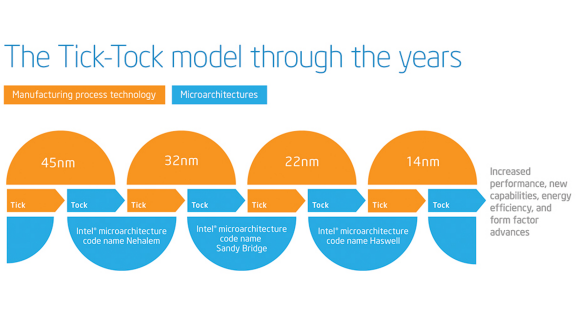
Multiple chip development methodologies have surfaced but the blockbuster approach, which took Intel Corporation to the insane heights of the success, was the renowned “Tick-Tock” approach. Over the years, it held strong dominance but the days of the famous Tick-Tock strategy have finally met their end and now the American chipmaker had finally taken decision to say goodbye to its microprocessor supremacy’s foundation.
Before 2007, Intel was deprived of a coherent, predictable, and definite placement linking the implementation, at smaller process nodes, of novel manufacturing techniques and the introduction of the latest architectures. After the deployment of the long running Tick-Tock strategy, the chipmaker was finally able to fix the area in which it was lagging behind and it issued the new process nodes, which were named as “ticks,” whereas the novel architectures were built on the exact process node and called “tocks.”
Nevertheless, the strategic era has finally ended when the Santa Clara, Calif. firm announced that it is transitioning to Process-Architecture-Optimization (PAO) – a three-step development process. This latest transition was not much surprising as last year. In 2015, Intel had already hinted about the slumping performance of the 10-nanometer technology and declared that the technology’s production is less likely to happen by the end of the year.
The year old anticipation of the company was finally transferred into a reality after Intel finally declared the expiration of the technology in its latest 10-K filing. The chipmaker cited that the company is working to expand the length of time during which its 14 nanometer could easily be utilized. It expects that the 10-nanometer next-gen process technologies will optimize chipmaker’s product and process technologies while simultaneously reaching the “yearly market cadence for product introductions.”
The probable plans of introducing several product families were also highlighted in the filing. The company stated it looks forward to launch a third 14nm product, dubbed as “Kaby Lake.” The latest addition is likely to have chief performance enhancements in comparison to the chipmaker’s 6th generation processor family. The company also discloses the futuristic production of 10nm manufacturing process technology, which is more likely to be market as the company’s next-gen process technology.
It will be too early to have an opinion whether the new methodology of chip development will be able to cater to the favorable impact or to imitate the Tick-Tock strategy success but the semiconductor manufacturing company is positively hopeful about the improvements the new technology will bring into different areas that will subsequently provide better user experience. The time will be the judge whether the chipmaker took a wise decision after all.